Integrated circuits
by Chris Woodford. Last updated: July 3, 2023.
Have you ever heard of a 1940s computer called the ENIAC? It was about the same length and weight as two to three double-decker buses and contained 18,000 buzzing electronic switches known as vacuum tubes. Despite its gargantuan size, it was about a billion times less powerful than a modern laptop—a machine about 1500 times smaller. [1]
If the history of computing sounds like a magic trick—squeezing more and more power into less and less space—it is! What made it possible was the invention of the integrated circuit (IC) in 1958. It's a neat way of cramming hundreds, thousands, millions, or even billions of electronic components onto tiny chips of silicon no bigger than a fingernail. Let's take a closer look at ICs and how they work!
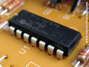
Photo: An integrated circuit from the outside. This one comes in a convenient form called a dual-inline package (DIP), which consists of a black plastic or ceramic outer case with metal pins down each side for plugging into a bigger electronic circuit board (the brown thing you can see in the background). The actual circuit that does the work is a tiny little chip embedded inside the DIP; you can see how it's connected to the DIP's outer pins in the next photo.
Sponsored links

Contents
What is an integrated circuit?
Open up a television or a radio and you'll see it's built around a printed circuit board (PCB): a bit like an electric street-map with small electronic components (such as resistors and capacitors) in place of the buildings and printed copper connections linking them together like miniature metal streets.
Circuit boards are fine in small appliances like this, but if you try to use the same technique to build a complex electronic machine, such as a computer, you quickly hit a snag. Even the simplest computer needs eight electronic switches to store a single byte (character) of information. So if you want to build a computer with just enough memory to store this paragraph, you're looking at about 750 characters times 8 or about 6000 switches—for a single paragraph! If you plump for switches like they had in the ENIAC—vacuum tubes about the size of an adult thumb—you soon end up with a whopping great big, power-hungry machine that needs its own mini electricity plant to keep it running.

Photo: "Electric street-map": An integrated circuit (right) on a printed circuit board (PCB) with various conventional electronic components.
When three American physicists invented transistors in 1947, things improved somewhat. Transistors were a fraction the size of vacuum tubes and relays (the electromagnetic switches that had been replaced by vacuum tubes in the mid-1940s), used much less power, and were far more reliable. But there was still the problem of linking all those transistors together in complex circuits. Even after transistors were invented, computers were still a tangled mass of wires.
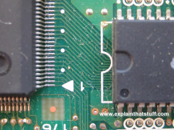
Photo: Integrated circuits fit into printed circuit boards (PCBs) like the green one you can see here. Notice the thin tracks linking the "legs" (terminals) of two different ICs together. Other tracks link the ICs to conventional electronic components such as resistors and capacitors. You can think of the tracks as "streets" making paths between "buildings" where useful things are done (the components themselves). There's also a miniaturized version of a circuit board inside an integrated circuit: the tracks are created in microscopic form on the surface of a silicon wafer.
Integrated circuits changed all that. The basic idea was to take a complete circuit, with all its many components and the connections between them, and recreate the whole thing in microscopically tiny form on the surface of a piece of silicon. It was an amazingly clever idea and it's made possible all kinds of "microelectronic" gadgets we now take for granted, from digital watches and pocket calculators to Moon-landing rockets and missiles with built-in satellite navigation.
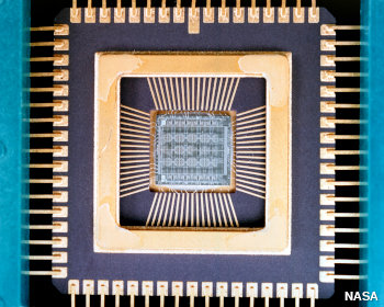
Photo: An integrated circuit from the inside. If you could lift the cover off a typical microchip like the one in the top photo (and you can't very easily—believe me, I've tried!), this is what you'd find inside. The integrated circuit is the tiny square in the center. Connections run out from it to the terminals (metal pins or legs) around the edge. When you hook up something to one of these terminals, you're actually connecting into the circuit itself. You can just about see the pattern of electronic components on the surface of the chip itself. Photo by courtesy of NASA Glenn Research Center (NASA-GRC) and Internet Archive.
Moore's Law
Integrated circuits revolutionized electronics and computing during the 1960s and 1970s. First, engineers were putting dozens of components on a chip in what was called Small-Scale Integration (SSI). Medium-Scale Integration (MSI) soon followed, with hundreds of components in an area the same size. Predictably, around 1970, Large-Scale Integration (LSI) brought thousands of components, Very-Large-Scale Integration (VLSI) gave us tens of thousands, and Ultra Large Scale (ULSI) millions—and all on chips no bigger than they'd been before.
In 1965, Gordon Moore (1929–2023) of the Intel Company, a leading chip maker, noticed that the number of components on a chip was doubling roughly every one to two years. Moore's Law, as this is known, has continued to hold ever since. Interviewed by The New York Times 50 years later, in 2015, Moore revealed his astonishment that the law has continued to hold:
"The original prediction was to look at 10 years, which I thought was a stretch. This was going from about 60 elements on an integrated circuit to 60,000—a thousandfold extrapolation over 10 years. I thought that was pretty wild. The fact that something similar is going on for 50 years is truly amazing."
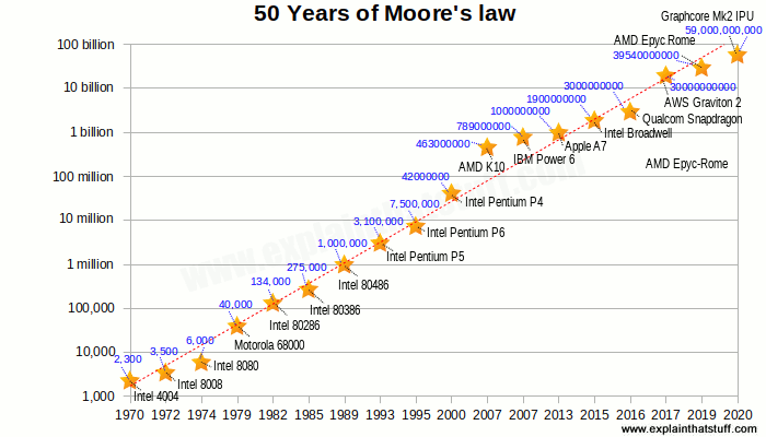
Chart: Moore's Law: The number of transistors packed into microchips has roughly doubled every year or two for the last five decades—in other words, it's grown exponentially. If you plot the number of transistors (y-axis) against the year of launch (x-axis) for some common microchips from the last few decades (yellow stars), you'll get an exponential curve; plotting the logarithm instead, you'll get this straight line. Please note that the vertical (y) axis of this chart is logarithmic and (due to the OpenOffice graphing software I used) the horizontal (x) axis is only vaguely linear. Source: Plotted using data from Transistor Count, Wikipedia, checked against other sources.
How are integrated circuits made?
How do we make something like a memory or processor chip for a computer? It all starts with a raw chemical element such as silicon, which is chemically treated or doped to make it have different electrical properties...
Doping semiconductors
If you've read our articles on diodes and transistors, you'll be familiar with the idea of semiconductors. Traditionally, people thought of materials fitting into two neat categories: those that allow electricity to flow through them quite readily (conductors) and those that don't (insulators). Metals make up most of the conductors, while nonmetals such as plastics, wood, and glass are the insulators.
In fact, things are far more complex than this—especially when it comes to certain elements in the middle of the periodic table (in groups 14 and 15), notably silicon and germanium. Normally insulators, these elements can be made to behave more like conductors if we add small quantities of impurities to them in a process known as doping. If you add phosphorus (or antimony) to silicon, you give it slightly more free electrons than it would normally have—and the power to conduct electricity. Silicon "doped" that way is called n-type. Add boron instead of phosphorus and you remove some of silicon's free electrons, leaving behind "holes" that work as "negative electrons," carrying a positive electric current in the opposite way. That kind of silicon is called p-type. Putting areas of n-type and p-type silicon side by side creates junctions where electrons behave in very interesting ways—and that's how we create electronic, semiconductor-based components like diodes, transistors, and memories.

Photo: Integrated circuits are manufactured in scrupulously clean conditions; workers have to wear "bunny suits" like this to stop them contaminating the chips they're making. This is Intel's wafer fabrication plant in Chandler, Arizona, USA. Photo courtesy of Carol M. Highsmith Archive, Library of Congress, Prints and Photographs Division.
Inside a chip plant
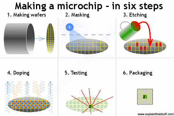
The process of making an integrated circuit starts off with a big single crystal of silicon, shaped like a long solid pipe, which is "salami sliced" into thin discs (about the dimensions of a compact disc) called wafers.
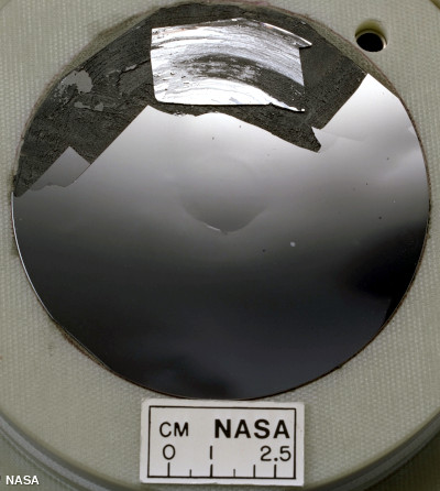
Photo: A silicon wafer. Photo by courtesy of NASA Glenn Research Center (NASA-GRC) and Internet Archive.
The wafers are marked out into many identical square or rectangular areas, each of which will make up a single silicon chip (sometimes called a microchip). Thousands, millions, or billions of components are then created on each chip by doping different areas of the surface to turn them into n-type or p-type silicon. Doping is done by a variety of different processes. In one of them, known as sputtering, ions of the doping material are fired at the silicon wafer like bullets from a gun. Another process called vapor deposition involves introducing the doping material as a gas and letting it condense so the impurity atoms create a thin film on the surface of the silicon wafer. Molecular beam epitaxy is a much more precise form of deposition.
Of course, making integrated circuits that pack hundreds, millions, or billions of components onto a fingernail-sized chip of silicon is all a bit more complex and involved than it sounds. Imagine the havoc even a speck of dirt could cause when you're working at the microscopic (or sometimes even the nanoscopic) scale. That's why semiconductors are made in spotless laboratory environments called clean rooms, where the air is meticulously filtered and workers have to pass in and out through airlocks wearing all kinds of protective clothing.